NVIDIA Introduces NVHBM Technology to Boost High-Bandwidth Memory Efficiency by 30 Percent
NVIDIA has unveiled NVHBM, a custom high-bandwidth memory technology that integrates the memory controller directly into the HBM base die to deliver up to 30 percent higher bandwidth and 15 percent lower power consumption than standard HBM4E.
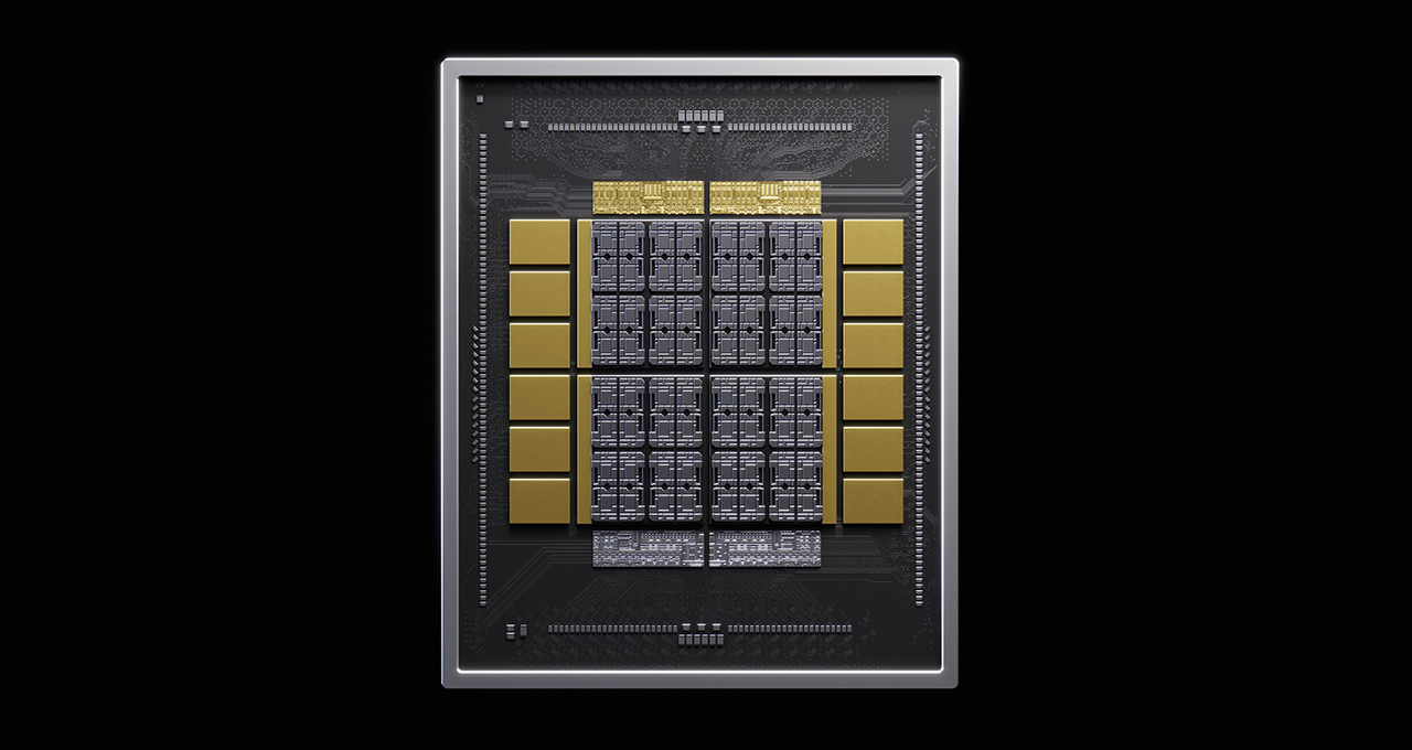
NVIDIA has announced a next-generation high-bandwidth memory technology called NVHBM, designed to scale its NVLink Fusion interconnect technology for semi-custom AI infrastructure. By targeting hyperscalers developing proprietary XPU accelerators, this architecture aims to alleviate memory bandwidth bottlenecks common in large language models and advanced AI workloads. Annapurna Labs, an Amazon subsidiary, is the first major partner planning to validate and adopt this technology for its custom silicon.
Primary source
Open NVIDIA ↗This article summarizes the source. Check the original for full details and conditions.
Comparison
| Aspect | Before / Alternative | After / This |
|---|---|---|
| Memory Controller Location | Positioned on the primary XPU compute die | Integrated into the 3D-stacked HBM base die |
| XPU Compute Die Area | Occupied by controller logic, reducing space for processing units | Saves up to 25% of die area, allowing more space for compute cores |
| Energy Efficiency | Baseline power consumption of standard HBM4E designs | Power consumption reduced by 15% compared to standard HBM4E |
| System Integration | Separated memory and processing development paths | Unified design approach treating memory and processing as a single unit |


